La plateforme Européenne de microscopie électronique en transmission effectue des recherches indépendantes ainsi que des travaux de service pour les académiques et les industriels. La plateforme est certifiée ISO 9001.
La plateforme de microscopie électronique en transmission “E-TEM” est membre du réseau national de microscopie électronique et sonde atomique (METSA) et ouvert pour les utilisateurs externes des universités, des instituts de recherche et de l’industrie.
Contact :
Dris IHIAWAKRIM – Responsable Technique
dris.ihiawakrim@ipcms.unistra.fr
+33 (0)3 88 10 70 15
Ovidiu ERSEN – Responsable Scientifique
ovidiu.ersen@ipcms.unistra.fr
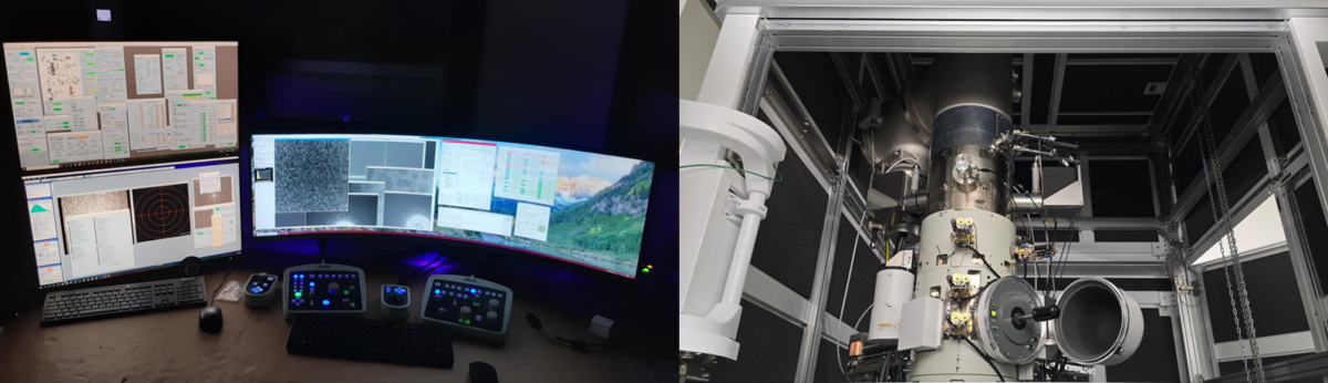
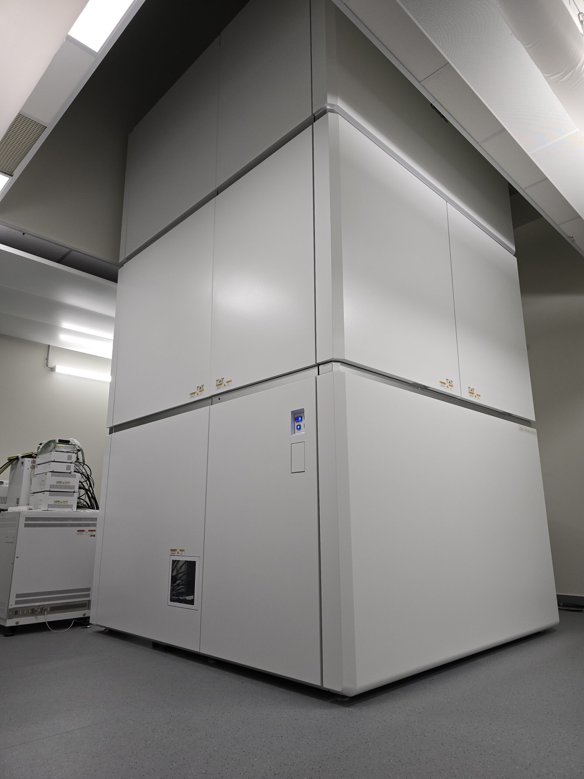
Three transmission electron microscopes (JEOL Grand ARM300F2 (OPERANDO), JEOL 2100F Cs Corrected, and JEOL 2100 LaB6) are currently in operation, supported by a comprehensive range of advanced peripherals including dedicated specimen holders for in-situ experiments (liquid, gas, and electrochemistry), electron tomography, and a full suite of specimen preparation tools. A broad spectrum of nanocharacterization techniques is available, such as high-resolution TEM imaging, scanning TEM (STEM), electron diffraction, EELS, EDX, and 3D electron tomography. The facility places a strong emphasis on in-situ electron microscopy and operando analysis, where numerous in-house and collaborative research projects are conducted. The new JEOL Grand ARM300F2, unique in France, offers sub-angstrom resolution, enhanced analytical capabilities, and is central to the platform’s methodological developments in environmental and 3D microscopy.


Formation CNRS : La tomographie électronique – théorie et pratique
Instrumentation
Transmission electron microscopes
– Operando TEM : JEOL Grand ARM300F2, 300 kV (80kV and 60kV), sub-angstrom resolution, TEM aberration corrector, two direct detection cameras, dual EDS detectors, EELS, and energy-filtered TEM (EFTEM). It also includes an integrated light system and an OBF detector, enabling high-resolution structural and chemical analysis under real-time, operando conditions. This unique combination of capabilities makes it a one-of-a-kind instrument in France for advanced materials research.
– JEOL 2100F (200 kV, Cs-corrected condenser, imaging filter, EDX, biprism, 2 CCD cameras)
– JEOL 2100 LaB6 (200 kV, EDX, CCD camera)
Specimen stages
– single and double tilt – tomography (+/- 80°) – heating (< 1000°C) – cooling (liq. N2) – STM Nanofactory
Specifications of the instrumentation
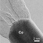
– image resolution in STEM: 0.11 nm – image resolution in TEM: 0.2 nm – energy resolution in EELS: 0.7 eV – tilt range for tomography: +/- 80° – specimen temperature range: -190 – 1000°C
Specimen preparation facilities
– mechanical grinding, cutting, dimpling etc. – ion milling – chemical preparation
Techniques
– scanning transmission electron microscopy STEM – in-situ electron microscopy – electron tomography – electron energy-loss spectroscopy EELS – electron diffraction – electron holography
Applications
– Independent research projects of the platform are carried out in the fields of: – carbon nanomaterials (graphene, nanotubes) – nanocomposites (carbon-metal nanoparticles) – atomic defects in nanomaterials – interfaces in nanomaterials – nanoparticles in catalysis
Services Work
for other groups concentrates on (at present): – spintronics – inorganic materials – catalysis
Education
Electron microscopy is now part of regular courses for the bachelor and master level in physics at the University of Strasbourg. Courses are also held for the PhD school (Ecole Doctorale de Physique) in Strasbourg. Several PhD students carry out their research dedicated to electron microscopy.