Current induced domain wall states in CPP nanopillars with perpendicular anisotropy D. Ravelosona (IEF, Orsay), S. Mangin (LPM, Nancy), Y. Henry, Y. Lemaho, J. A. Katine, B. D. Terris, and Eric E. Fullerton (Hitachi GST, San Jose) JOURNAL OF PHYSICS D-APPLIED PHYSICS 40, 253 (2007)
Current induced domain wall creation in CPP-GMR nanopillars made of Co/Ni films with strong perpendicular magnetic anisotropy is described. We find that stable domain wall states (DWS) can be nucleated with modest current densities of ∼ 107 A.cm−2 and further controlled by current to restore the two uniform states. The reproducibility of both the creation and annihilation of such DWS is studied. Experiments have been performed several times for a given nanopillar, but also for different devices. The influence of temperature, size and shape of the devices, as well as the distribution of magnetic properties on magnetization reversal is discussed.
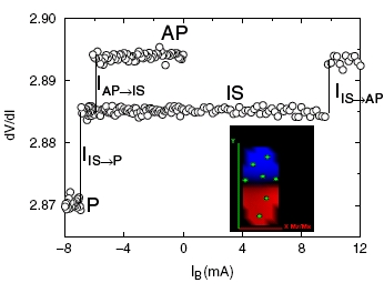
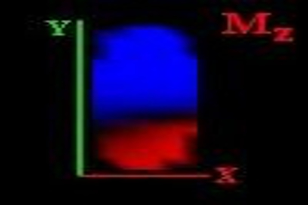
Fig. 1 : Differential resistance as a function of current for a 100 nm × 200 nm pillar. The effective magnetic field acting on the magnetization of the free layer is almost nil. The initial state is the antiparallel (AP) state. The current sweeps from the AP to the intermediate state (IS) and then back to the AP state. The transition from the IS to parallel (P) state is also shown. The inset corresponds to micromagnetic simulations (perpendicular component of the magnetization. The dots are a schematic illustration of the pinning sites.
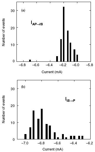
Fig. 2 : Distribution of critical current for the (a) AP → IS transition and (b) IS → P transition, for the device of figure 1, as obtained from 200 measurements.
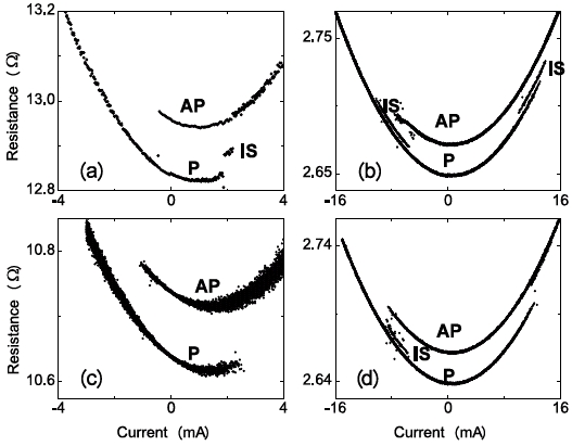
Fig. 3 : Resistance versus DC current loops for 4 different nanodevices : (a,c) 50 nm × 100 nm, (b,d) 100 nm × 200 nm. For each device, several loops are shown which correspond to effective field values between −500 Oe and +500 Oe. Current induced IS is not reproducible from device to device. The parabolic shape is due to Joule heating of the sample.