In a nanocrystal array, transport occurs though hopping mechanism, leading to limited carrier diffusion length, in the 10 to 100 nm range. In the case of HgTe nanocrystals, Lan et al. [1] recently proposed that transport actually occurs between island of strongly coupled nanocrystals. In other word, partly delocalize states are formed within these islands and the bottleneck for conduction becomes the link between these islands. Based on this idea, it becomes of utmost interest to probe transport at the scale of a single island where transport can efficiently occur.
IPCMS recently collaborated with Emmanuel Lhuillier team of INSP (Paris), together with ONERA (Gregory Vincent, Palaiseau) and IEMN (Christophe Delerue, Lille) to address this technological lock. [2]
The authors exploited a smart concept of “nanotrench” electrodes, previously introduced by Dayen et al. [3] and developed at StNano plateform, to build high aspect ratio electrodes spaced by few nanometers only and expanding over several tenths of µm. Device size resolution is no longer set by the wavelength of the light used for the lithography but rather by device geometrical factor, down to few nanometers resolution.
We observe that for such small devices the light responsivity of a thin film of HgTe nanocrystals exposed to infrared light is strongly enhanced compared to the same film deposited on µm-spaced electrodes. Because the device is small, gain is generated and quantum efficiency above 105 are achieved (corresponding to 105 electrons flowing per absorbed photons). This large gain enables large signal to noise ratio reaching 2×10¹² Jones at 200 K for a device with 2.5 µm cut-off wavelength, see figure 1b. This result over-performs the best photodiodes operating at the same wavelength. [2]
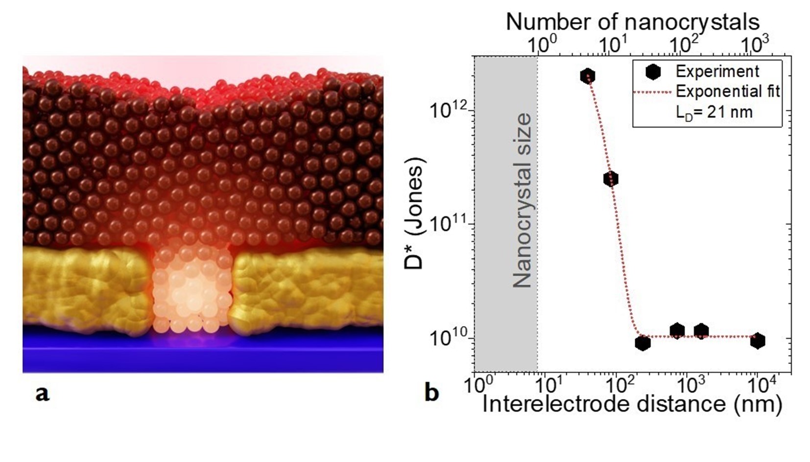
Carefull optoelectronics study and theoretical modeling demonstrates that transport is only driven by the part of the nanocrystal film located within the nanogap, and asset the top-notched performances of our device to the ultimate length scale of the photoactive channel. This result is important since it contradicts a common thought in the field that only photodiodes enable highest performances. The next challenge will be to achieve a matrix of such electrodes.
These result, published in Nature Communications, are important since it contradicts a common thought in the field that only photodiodes enable highest performances. The next challenge will be to achieve a matrix of such electrodes, and to address new generation of photovoltaic cells.
Read our article in https://www.nature.com/articles/s41467-021-21959-x
References
[1] Quantum dot solids showing state-resolved band-like transport, X. Lan et al., Nature materials 19, 323 (2020)
[2] Infrared photoconduction at the diffusion length limit in HgTe nanocrystal arrays. Chu, A., et al. Nat Commun 12, 1794 (2021). https://doi.org/10.1038/s41467-021-21959-x
[3] Nanotrench for nano and microparticle electrical interconnects, J-F. Dayen et al., Nanotechnology 21, 335303 (2010)