

In this work, we demonstrate a new type of device, a spin-filter tunnel transistor, built by stacking a few atomic layers of two-dimensional materials: two graphene electrodes separated by a thin layer of the antiferromagnetic semiconductor CrSBr, which acts as a spin-filtering barrier. This architecture, known as a van der Waals heterostructure, combines within only a few nanometers functionalities that cannot be integrated in conventional bulk materials.
We show that this device provides two independent electrical “knobs” to control spin filtering. First, the voltage applied across the electrodes tilts the tunnel barrier energy profile, dramatically enhancing the spin-filtering efficiency from only a few percent to several thousand percent. Second, a gate voltage, as in a conventional field-effect transistor, further modulates the spin-dependent transport signal. A theoretical model based on spin-dependent tunneling quantitatively reproduces these observations, while first-principles calculations validate the electronic structure underlying the device operation.
These findings pave the way toward fully electrical, reconfigurable spintronic circuits, in which a single device architecture could operate, depending on the applied voltages, as a memory element, a magnetic sensor, or a logic gate. More broadly, they highlight the tremendous potential of magnetic two-dimensional materials for the development of the next generation of quantum and ultra-low-power electronic devices.
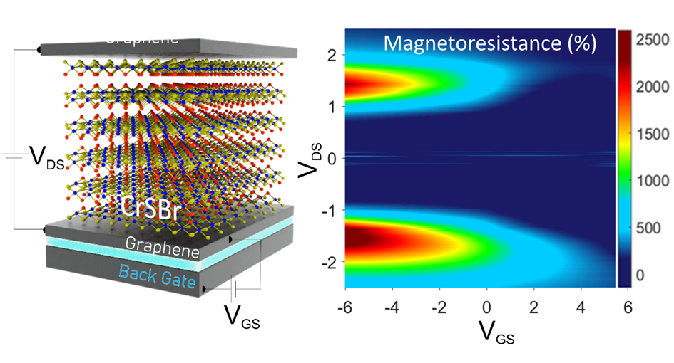
Figure : Gauche : Schéma du transistor tunnel à filtrage de spin. Une barrière tunnel de CrSBr (semiconducteur antiferromagnétique 2D) est intercalée entre deux électrodes de graphène. Droite : Les tensions source-drain et de grille contrôlent conjointement le filtrage du spin.
Copyright : ©[DAYEN Jean-Francois / IPCMS (CNRS / Université de Strasbourg)
Reference : ACS Nano (American Chemical Society), 07 Juillet 2026 , https://pubs.acs.org/doi/full/10.1021/acsnano.6c03448
Contact : Jean-François Dayen