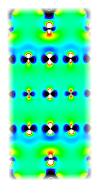
Decoding the Structure of a New Superconductor

Bilayer nickelates have recently emerged as one of the most exciting new families of superconductors, offering fresh opportunities to understand the mechanisms behind high-temperature superconductivity. Yet, reproducing superconductivity in thin films has proven extremely challenging, with seemingly similar samples often exhibiting strikingly different electronic properties. Understanding the origin of these discrepancies is a crucial step toward the reliable design of superconducting nickelate devices.

Researchers at IPCMS (CNRS–Université de Strasbourg) and LPS (Paris-Saclay) have taken an important step toward answering this question by studying a new family of materials known as bilayer nickelates, which recently attracted worldwide attention after superconductivity was discovered in them.

Using state-of-the-art electron microscopy and spectroscopy, the team investigated how subtle changes in the atomic structure and oxygen content influence the superconducting properties of ultrathin La3Ni2O7-δ films. Although samples can appear nearly identical using conventional structural characterization techniques, the researchers revealed that tiny variations in the stacking of atomic layers and the distribution of oxygen atoms can determine whether superconductivity appears or disappears.

One of the study’s most significant findings is the identification of a particular crystal stacking sequence that does not support superconductivity. This discovery helps explain why superconductivity in bilayer nickelate thin films has been notoriously difficult to reproduce and highlights the importance of precisely controlling both crystal structure and oxygen stoichiometry during fabrication. Beyond solving a long-standing materials challenge, the work provides practical guidelines for producing more stable superconducting nickelate thin films operating at ambient pressure. These insights bring scientists one step closer to designing and engineering a new generation of oxide superconductors for future electronic technologies.
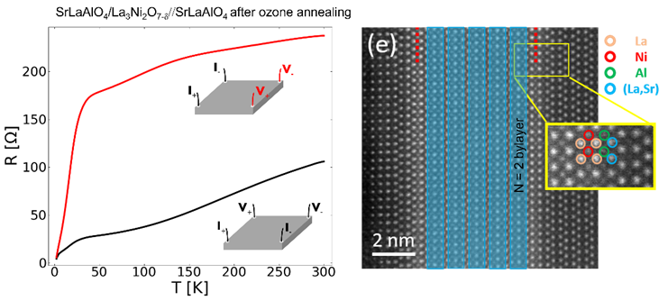
Reference : Flavenot Mathieu, Sahib Hoshang, Robert Jerome, Lenertz Marc, Versini Gilles, Schlur Laurent, Gloter Alexandre, Viart Nathalie, Preziosi Daniele, Decoding superconductivity in La3Ni2O7-d Thin Films via Ozone-Driven Structure and Oxidation Tuning, Small Structures 2026, 0, e70542. http://doi.org/10.1002/sstr.70542

Contact : Daniele.Preziosi@ipcms.unistra.fr
Infinite-layer nickelates: a new step towards understanding unconventional superconductivity

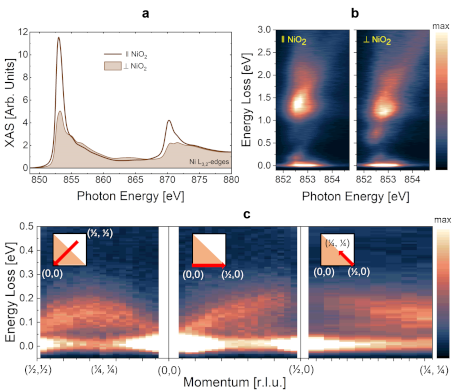
Using state-of-the-art resonant inelastic X-ray scattering (RIXS) at the European Synchrotron Radiation Facility (ESRF), researchers performed the most comprehensive comparison to date of the magnetic, electronic and orbital excitations in infinite-layer nickelates and cuprates. The results reveal that nickelates share many of the key ingredients underlying unconventional superconductivity in cuprates, while also displaying important differences that help explain why their superconducting transition temperatures remain significantly lower.

The study shows that magnetic interactions in nickelates are intrinsically weaker than in cuprates, reducing the energy scale available for superconducting pairing. In addition, the rare-earth ions present in nickelates introduce a self-doping mechanism and a more three-dimensional electronic structure, if compared to the infinite-layer cuprates. Together, those findings establish infinite-layer nickelates as a new family of unconventional superconductors closely related to cuprates, while identifying the microscopic factors that currently limit their performance.

This work is the result of a close collaboration between IPCMS (CNRS–Université de Strasbourg), Politecnico di Milano, the European Synchrotron Radiation Facility (ESRF) and CNR-SPIN in Napoli. By combining complementary expertise in oxides growth, advanced synchrotron spectroscopy and theoretical modelling, the collaboration provides important new insights into one of the central challenges of condensed matter physics: understanding the mechanisms behind high-temperature superconductivity.

The results not only deepen our understanding of nickelate superconductors but also provide valuable guidelines for the design of future quantum materials with enhanced superconducting properties.

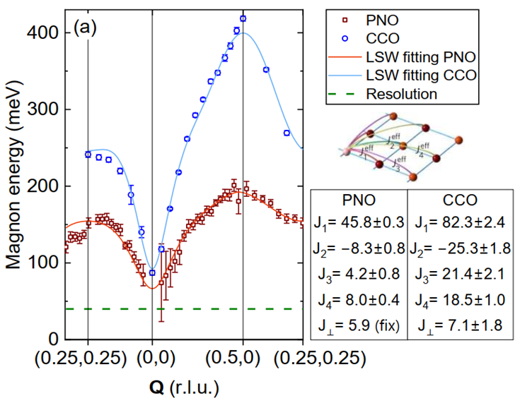
Figure 1 Fitting of dispersions of infinite layer nickelate PrNiO2 (PNO) and cuprate CaCuO2 (CCO) with the Linear Spin Wave (LSW) model fit. The definitions and values (in meV) of the four in-plane exchange coupling constants are displayed on the right.

Reference: Rosa, F., Sahib, H., Merzoni, G., Martinelli, L., Arpaia, R., Brookes, N. B., Castro, D. di, Wohlfeld, K., Zinouyeva, M., Salluzzo, M., Preziosi, D., & Ghiringhelli, G. (2026). Spin and orbital excitations in undoped infinite-layer superconducting PrNiO2 and insulating CaCuO2. Communications Materials. https://doi.org/10.1038/s43246-026-01266-y

Electrical control of spin filtering in a vertical tunnel transistor

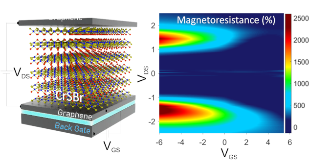
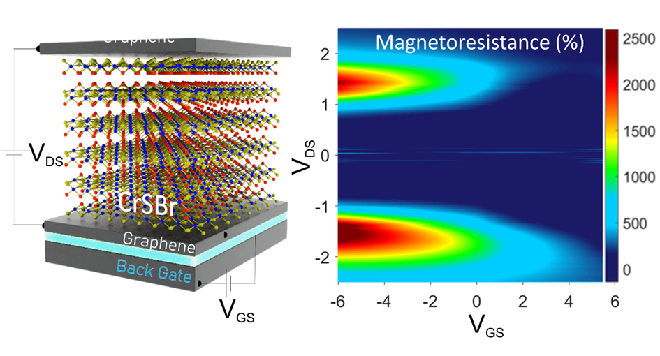
In this work, we demonstrate a new type of device, a spin-filter tunnel transistor, built by stacking a few atomic layers of two-dimensional materials: two graphene electrodes separated by a thin layer of the antiferromagnetic semiconductor CrSBr, which acts as a spin-filtering barrier. This architecture, known as a van der Waals heterostructure, combines within only a few nanometers functionalities that cannot be integrated in conventional bulk materials.

We show that this device provides two independent electrical “knobs” to control spin filtering. First, the voltage applied across the electrodes tilts the tunnel barrier energy profile, dramatically enhancing the spin-filtering efficiency from only a few percent to several thousand percent. Second, a gate voltage, as in a conventional field-effect transistor, further modulates the spin-dependent transport signal. A theoretical model based on spin-dependent tunneling quantitatively reproduces these observations, while first-principles calculations validate the electronic structure underlying the device operation.

These findings pave the way toward fully electrical, reconfigurable spintronic circuits, in which a single device architecture could operate, depending on the applied voltages, as a memory element, a magnetic sensor, or a logic gate. More broadly, they highlight the tremendous potential of magnetic two-dimensional materials for the development of the next generation of quantum and ultra-low-power electronic devices.

Figure : Gauche : Schéma du transistor tunnel à filtrage de spin. Une barrière tunnel de CrSBr (semiconducteur antiferromagnétique 2D) est intercalée entre deux électrodes de graphène. Droite : Les tensions source-drain et de grille contrôlent conjointement le filtrage du spin.
Copyright :  ©[DAYEN Jean-Francois / IPCMS (CNRS / Université de Strasbourg)

Reference : ACS Nano (American Chemical Society), 07 Juillet 2026 , https://pubs.acs.org/doi/full/10.1021/acsnano.6c03448

Contact : Jean-François Dayen

PEPR SPIN News

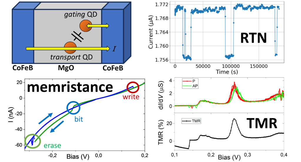
Scientists from IPCMS, the Institut Jean Lamour (CNRS/University of Lorraine), and the Institut de Chimie have reported in their paper, “MgO tunneling spintronics across capacitively-coupled atomic clusters,” the impact of carbon on spin-polarized electrical transport across microscale magnetic tunnel junctions.

Read the news on PEPR SPIN website

Reference : Nano Letters, 2025, 25 (52), pp.18026-18035. ⟨10.1021/acs.nanolett.5c03672⟩. ⟨hal-05457364⟩

Contact : Martin Bowen

Ferroelectric transitions under high pressure

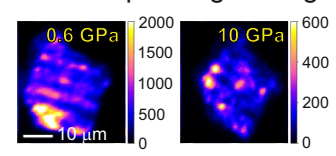
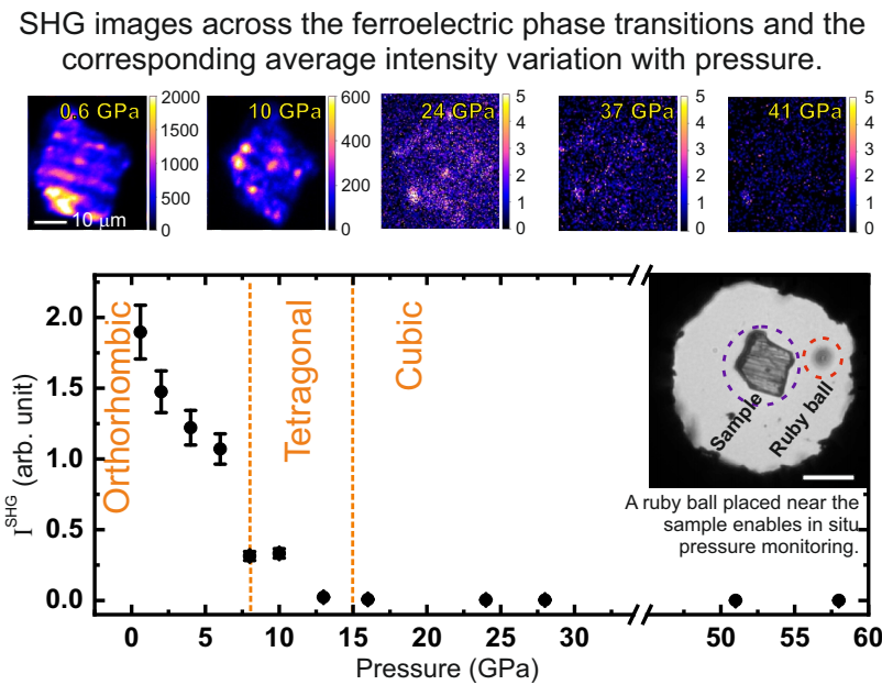
Using the same pressure cell, it enables experiments performed at large-scale synchrotron facilities to be combined with high-pressure optical measurements carried out in the laboratory, in particular using nonlinear optical microscopy. The device integrates in situ pressure measurement by fluorescence directly within a second-harmonic generation (SHG) microscope, allowing precise and continuous monitoring of experimental conditions. Its design and implementation rely on instrumental developments in optics, mechanics, and measurement methodology carried out at IPCMS. This setup made it possible to reveal ferroelectric phase transitions induced by hydrostatic pressure up to 60 GPa in KNbO₃, a reference ferroelectric perovskite. Published in Physical Review Letters, this work is the result of a collaboration between the University of Luxembourg, Institut Néel, and the synchrotrons SOLEIL and ESRF. It opens new perspectives for multimodal studies of ferroelectric materials under extreme conditions.

Référence

Shoker et al., Re-emergence of a Polar Instability at High Pressure in KNbO3, Phys. Rev. Lett. 136, 056101 (2026) https://doi.org/10.1103/vwp9-tr7b < hal-05206803>

Contact Boris Croes Boris.Croes@ipcms.unistra.fr (Postdoc, IPCMS)

Hydrogen atoms reveal interactions at the atomic scale in graphene

Read the news on “CNRS Physique” web site

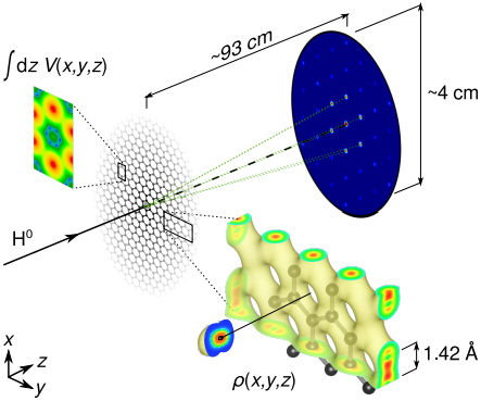
Schematic view of the modeling of coherent diffraction of a beam of hydrogen atoms through a sheet of graphene. © Pierre Guichard et al., 2025 American Physical Society

Reference :

Fast Hydrogen Atom Diffraction through Monocrystalline Graphene, Pierre Guichard, Arnaud Dochain, Raphaël Marion, Pauline de Crombrugghe de Picquendaele, Nicolas Lejeune, Benoît Hackens, Paul-Antoine Hervieux, Xavier Urbain, Physical Review Letters 135, 263403 – Publié le 23 décembre 2025.
DOI : 10.1103/wdx6-mrvm
Archive ouverte : arXiv

Contact

Paul-Antoine Hervieux (Enseignant-chercheur de l’Université de Strasbourg à l’Institut de physique et chimie des matériaux de Strasbourg (IPCMS)

paul-antoine.hervieux@ipcms.unistra.fr

Magnetoresistive detection of spin waves

Read the News on “CNRS Physique” Website

Référence :

Magnetoresistive detection of spin waves, Quentin Rossi, Daniel Stoeffler, Gregoire De Loubens, Hugo Merbouche, Hicham Majjad, Yves Henry, Igor Ngouagnia, Aurelie Solignac, Matthieu Bailleul, Science Advances 11, eadx4126 – Publié le 15 août 2025.
DOI : 10.1126/sciadv.adx4126
Archives ouvertes : HAL

Contacts : Quentin Rossi (Doctorant IPCMS-DMONS) : quentin.rossi@ipcms.unistra.fr

Matthieu Bailleul (Chercheur IPCMS- DMONS) : matthieu.bailleul@ipcms.unistra.fr

Optically generating a two-dimensional electron gas

Two-dimensional electron gases (2DEGs) are a fundamental element of modern electronics. Among the various systems capable of hosting them, complex oxide heterostructures stand out. In addition to offering very high electronic mobility, these systems allow for the exploitation of unique properties, such as spin-orbit coupling and strong electronic correlations. These features pave the way for new functionalities, while creating links to fields such as spintronics and photonics. In this context, the ability to manipulate 2DEGs using external stimuli is considered a holy grail. In this study, the researchers demonstrated the instant creation of a 2DEG at the interface between two oxides, where such an electronic state is otherwise absent, using light. This 2DEG disappears just as quickly once the light is turned off. The result is a giant photoconductance effect: under illumination, the electrical conductance is up to five orders of magnitude higher than in the dark! These effects were observed at the interface between thin layers of Nd₁₋ₓSrₓNiO₂ (x = 0, 0.05, and 0.2) and their SrTiO₃ substrate.

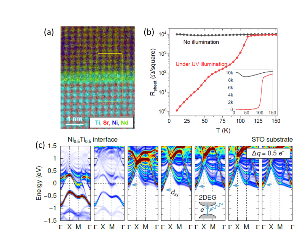
To achieve these results, the researchers first epitaxially deposited ultrathin layers of the perovskite Nd₁₋ₓSrₓNiO₃ (x = 0, 0.05, and 0.2) on SrTiO₃ using pulsed laser deposition. Then, a topotactic reduction process allowed them to obtain the infinite-layer phase of Nd₁₋ₓSrₓNiO₂. Transport measurements under ultraviolet and visible light revealed photoconductance effects and their dependence on photon energy. To uncover the microscopic mechanisms responsible for the generation of the 2DEG, the team combined an in-depth study of the interface using transmission electron microscopy (4D-STEM) and electron energy loss spectroscopy (EELS) with advanced density functional theory calculations. They highlighted that the key factors for generating the 2DEG are the structural and electronic reconstructions at the NdNiO₂//SrTiO₃ interface, as well as the presence of an intrinsic interfacial electric field. This field promotes the occupation of the high-mobility Ti-3dxy conduction band by photoexcited electrons, drawing them toward the interface and separating them from the holes left in the Ti valence band. These results are very interesting, both from a fundamental perspective and for their potential applications. On the one hand, they reveal how slight variations in the electronic structure at the interface – whether related to atomic layer terminations, local oxidation states, or temperature – can significantly modulate the confinement and distribution of photo-generated carriers in the interfacial bands. On the other hand, this refined understanding of the underlying microscopic mechanisms opens up promising perspectives for engineering the photo-response of strongly correlated electrons. Among the potential applications, one can consider, for example, the optical control of the superconducting state in infinite-layer nickelates.

The work presented in this article is the result of collaboration between several laboratories in France (LAF, IPCMS, LPS, SOLEIL), Germany (University of Duisburg-Essen), Spain (Universidad Complutense de Madrid), and the United States (University of Florida). This work is part of a broader effort at CNRS, dedicated to manipulating electronic states with light in strongly correlated oxides and their heterostructures, including superconductors, spintronic and electronic materials, within the EIC Pathfinder projects “JOSEPHINE” and “SPINMAT” under the PEPR SPIN program.

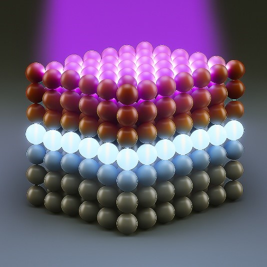
Figure 1: Representation of the photo generation of a two-dimensional electron gas at the interface between two oxides

Figure 2 (a) Transmission electron microscopy image combined with electron energy loss spectroscopy of an NdNiO₂//SrTiO₃ heterostructure. (c) Electrical resistance vs. temperature under illumination and in the dark, showing the giant photoconductance effect. (d) Energy bands and Fermi level at the interface and in several atomic planes from it, calculated by density functional theory

Reference : Giant photoconductance at infinite-layer nickelate/SrTiO3 interfaces via an optically induced high-mobility electron gas.
D. Sanchez-Manzano, G. Krieger, A. Raji, B. Geisler, V. Humbert, H. Jaffrès, J. Santamaría, R. Pentcheva, A. Gloter, D. Preziosi et Javier E. Villegas. Nature Materials, le 10 octobre 2025

Contacts :

Javier VILLEGAS, Laboratoire Albert Fert, CNRS, Thales, Université Paris-Saclay (javier.villegas@cnrs-thales.fr)

Daniele PREZIOSI, Institut de Physique et de Chimie des Matériaux de Strasbourg (daniele.preziosi@ipcms.unistra.fr)

Alexandre GLOTER, Laboratoire de Physique de Solides, Université Paris-Saclay (alexandre.gloter@universite-paris-saclay.fr)

You can also read the “Actualité” on CNRS Physique website