STnano facility is member of the National Network of Nanotechnology facilities. The platform has a dedicated 180 m2 ISO class 6 cleanroom area, including several ISO class 5 workspaces. A laboratory dedicated to electron beam lithography completes the platform. The platform has currently all the equipment for the nanofabrication of devices down to several tens of nanometers. STnano staff trains more than 30 users annually. STnano is a certified ISO 9001 : 2015 platform
User’s Guide STnano
This document is in French, if you need the English version please send an email to hicham.majjad@ipcms.unistra.fr
Project Form
All the group leaders who need an access to STnano facility for their research project have to fill a form describing briefly the project. STnano staff will check the technical feasibility and compatibility with running processes. The form should be sent to hicham.majjad@ipcms.unistra.fr
Fiche de demande de projet STnano
All participants to the project have to pay processing fees (Fees depends on user’s category and kind of activity, you will get a cost estimate) and sign the
STnano Services to companies and laboratories :
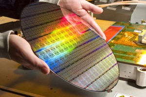
« Courtesy of International Business Machines Corporation »
STnano provides access to optical and e-beam lithography techniques, thin film deposition by evaporation, dry and wet etching on all types of substrates from 10 to 100 mm. The platform is equipped with latest generation equipment for nanofabrication and characterization (Oxford Instrument, Zeiss, Suss Microtec …).
- Metallic thin films evaporation (Au, Cu, Al, Ni, Co, …)
- Dielectric thin films evaporation (SiO2, Si3N4, Al2O3)
- Deep reactive etching (RIE-ICP)
- Oxygen plasma treatment
- Back end (AFM, wirebonding, 3D profilometry …)
STnano offers specialized training programs for technical staff and scientists in both industry and academic research. The platform welcomes partnerships, providing opportunities to collaborate on cutting-edge nanotechnology projects. With the guidance of highly skilled engineers, STnano supports your project from initial design stages through to proof of concept, ensuring a seamless process in developing innovative nanotechnology solutions.
Research Projects :
The projects aim to combine the bottom-up and top-down strategies at the nanoscale level. Different areas of physics and chemistry, and their interconnection, are concerned with scales of 500 nm in plasmonics, 100 nm in nanomagnetism and 10 nm to 1 nm for 2D materials and molecular materials. Research teams using the STnano platform work on different fields, including:
- Spintronics
- Nanomagnetism
- 2D materials
- Molecular Electronics
- Plasmonics
- Microfluidics
Around 20 running projects are using STnano facility.
5nm nanogap for molecular electronic
Propagating spin-wave spectroscopy device
Epitaxial MgO deposition on graphene for tunnel junctions fabrication
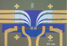
Optical microscopy image of and organic field emission transistor device, including extra electrodes for conductivity and Hall voltage measurements.
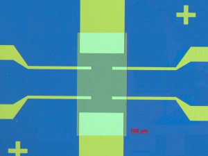
nanotranchées pour l’adressage de micro et nanoparticules

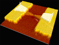
Magnetic force field between two Ni électrodes under a vertical external field. Source : C. Andreas, R. Hertel.
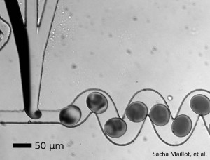
Microfluidic chip for reagents mixing
Teaching:
STnano is deeply committed to education and offers a variety of hands-on learning opportunities for Master’s and PhD students at Strasbourg University. Through specialized courses, practical lab work, and semester-long projects in its innovative “Student Lab,” Plaano equips students with crucial experience in nanofabrication tools and processes used in both industry and academic research.
In addition to student training, STnano also provides advanced training programs for technical staff and scientists from industrial and academic sectors, fostering expertise in cutting-edge nanotechnology techniques.
Contact :