Explications avec Paul-Antoine Hervieux, membre de la collaboration et enseignant-chercheur à l’Institut de physique et chimie des matériaux de Strasbourg (IPCMS – CNRS/Unistra).
“CORELMAG” fait partie des projets ANR 2019 : Nanocomposites innovants libérant des facteurs biologiques par hyperthermie magnétique en tant que composants de matrices intelligentes pour l’ingénierie tissulaire.
Coordinateur du projet : Damien MERTZ (IPCMS – DCMI)
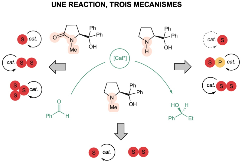
Divergence of catalytic systems in the zinc-catalysed alkylation of benzaldehyde mediated by chiral proline-based ligands. Thibault Thierry, Yannick Geiger & Stéphane Bellemin-Laponnaz Nature Synthesis2024 DOI https://doi.org/10.1038/s44160-024-00491-y
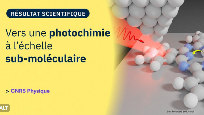
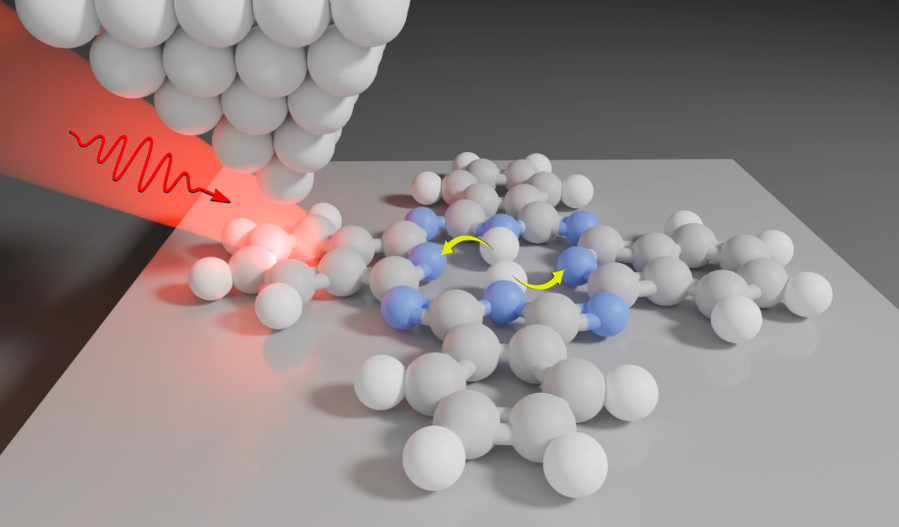
The article recently published in Nature Nanotechnology (Doi : 10.1038/s41565-024-01622-4): Submolecular-scale control of phototautomerization / Anna Roslawska, Katharina Kaiser, Michelangelo Romeo, Eloïse Devaux, Fabrice Scheurer, Stéphane Berciaud, Tomas Neuman and Guillaume Schull, is the subject of a news item on the CNRS Physique website.
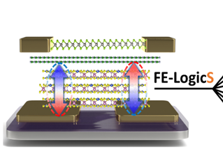
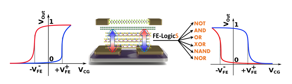
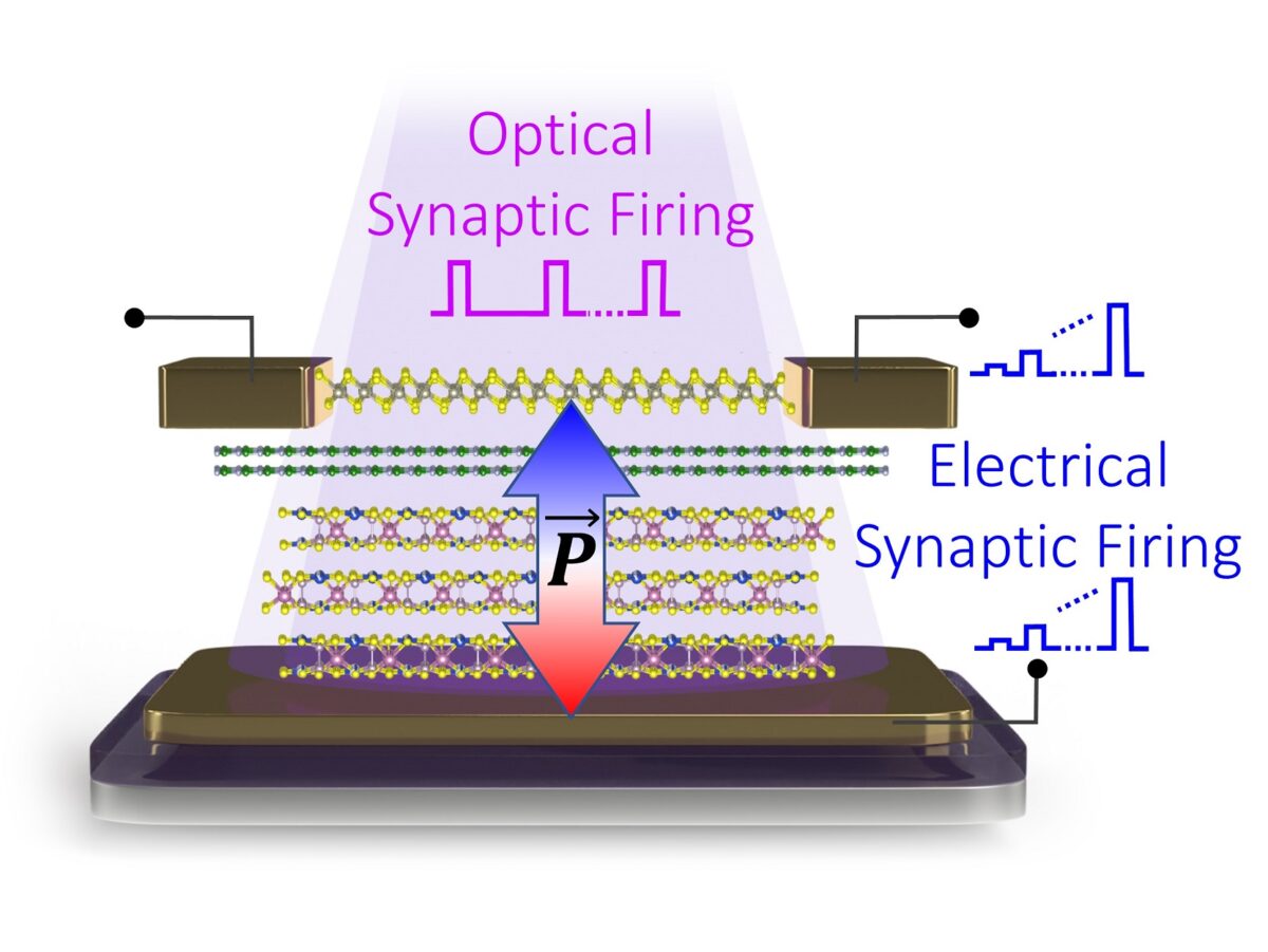
An international consortium (University of Strasbourg, University of Luxembourg, NIMS Japan, Ecole Centrale Lyon, C2N Saclay) led by IPCMS (team of Jean-François Dayen, DMONS), established the concept for a new generation of reconfigurable ferroelectronic logic circuits.
These devices, referred as Re-FeFET, allow for encoding and manipulating the information in a single operating unit, circumventing the famous ”Memory Wall” limitation of modern CMOS technology. By making use of the switchable polarization state of two ferroelectric gates, the electrical potential landscape within a semiconductor channel can be permanently and reconfigurably modified. Depending on the ferroelectric state encoded, the ferroelectric logic circuits can function as six alternative logic gates, while CMOS circuit are limited to a single function. Last but not least, the device can operate as a photodiode and generate photovoltaic energy. These findings rethink circuit topology and memory-logic interaction, opening up new research directions in the area of frugal computational enhancement.
Reference : Reconfigurable Multifunctional van der Waals Ferroelectric Devices and Logic Circuits Ankita Ram, Krishna Maity, Cédric Marchand, Aymen Mahmoudi, Aseem Rajan Kshirsagar, Mohamed Soliman, Takashi Taniguchi, Kenji Watanabe, Bernard Doudin, Abdelkarim Ouerghi, Sven Reichardt, Ian O’Connor and Jean-Francois Dayen. ACS Nano 2023, 10.1021/acsnano.3c07952. Link.
Schematic of a reconfigurable ferroelectric device, based on van der Waals materials, that can operate several logic functions within a single circuit.
Reconfigurable Multifunctional van der Waals Ferroelectric Devices and Logic Circuits, Ankita Ram, Krishna Maity, Cédric Marchand, Aymen Mahmoudi, Aseem Rajan Kshirsagar, Mohamed Soliman, Takashi Taniguchi, Kenji Watanabe, Bernard Doudin, Abdelkarim Ouerghi, Sven Reichardt, Ian O’Connor et Jean-Francois Dayen, ACS Nano, publié le 21 octobre 2023. Doi : 10.1021/acsnano.3c07952 Archives ouvertes : HAL
Une part importante des efforts de recherche en technologies de l’information essaie de contourner le goulot d’étranglement entre processeur et mémoire. Le premier doit travailler de plus en plus vite et manipuler toujours plus de données, alors que la vitesse d’échange avec les composants mémoire est limitée. Ainsi, les processeurs de nos ordinateurs passent une grande partie de leur temps à attendre… Une stratégie de recherche consiste à explorer des technologies « non-Von Neumann », orthogonales à cette architecture classique qui atteint ses limites.
Pour cela, une voie possible est celle des puces neuromorphiques, visant à s’inspirer des réseaux de neurones biologiques. Cette technologie, dite ‘In-memory computing’, permet d’exécuter à la fois des calculs et le stockage mémoire, au sein d’un même composant.
L’équipe Nanodevices de l’IPCMS, en collaboration avec le C2N (Saclay), vient de démontrer qu’une telle technologie neuromorphique pouvait être réalisée en combinant des couches ferroélectriques et semiconductrices de van der Waals. Intégrées dans une architecture de photo-transistor, un état de conductivité rémanent (non volatile) a pu être manipulé à la fois par des pulses électriques et optiques. Les excitations optoélectriques permettent de moduler de façon sélective l’équilibre entre la densité de charges d’interface ferroélectrique/semiconducteur, et le champ interne du ferroélectrique. En retour, la dynamique des domaines ferroélectrique est modifiée, permettant de contrôler l’état de polarisation ferroélectrique, lequel détermine l’état de conduction du FeFET.
Les chercheurs ont ainsi démontré la plasticité hétéro-synaptique de ces hétérostructures, en faisant fonctionner leur dispositif dans trois modes synaptiques différents : synapse stimulée électriquement, stimulée optiquement et assistée optiquement. Les réseaux de neurones artificiels simulés démontrent un excellent niveau de précision de 91 % proche du modèle idéal des synapses.
Ces résultats éclairent d’un jour nouveau la compréhension des mécanismes photo-ferroélectriques, laquelle est au cœur des enjeux du domaine. Ils permettent d’avancer vers une étape supplémentaire, l’intégration des systèmes ferroélectrique dans la feuille de route des prochaines architectures informatiques neuromorphiques.
Référence : Tip-induced excitonic luminescence nanoscopy of an atomically resolved van der Waals heterostructure, Luis E. Parra López, Anna Rosławska, Fabrice Scheurer, Stéphane Berciaud & Guillaume Schull, Nature materials, paru le 16 mars 2023 DOI : 10.1038/s41563-023-01494-4 Archive ouverte arXiv
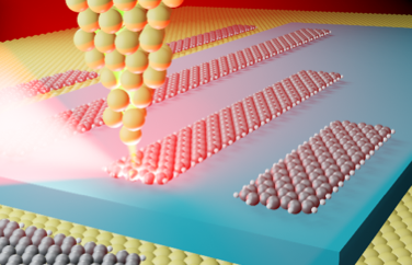
La fluorescence de nanorubans de graphène (GNR) synthétisés sur une surface métallique est étudiée avec une résolution spatiale sub-nanométrique en utilisant un microscope à effet tunnel (STM). L’émission de lumière observée implique des états topologiques qui se comportent comme des centres fluorescents localisés aux extrémités des GNR.
Depuis leur première synthèse, les nanorubans de graphène (GNR) ont suscité un intérêt considérable dans les communautés des nanosciences et nanotechnologies en raison de propriétés physiques uniques liées à leur topologie. En effet, la conformation spécifique de leurs bords est à l’origine d’états électroniques singuliers qui, à leur tour, conduisent à des propriétés de transport ou magnétiques particulières. Plusieurs études théoriques traitent en détail de la façon dont les propriétés optiques des GNR peuvent être avantageusement contrôlées par des variations à l’échelle atomique de leur largeur, de leur longueur et de la forme de leurs bords. Toutefois, les expériences portant sur les propriétés de fluorescence des GNR sont rares et limitées à des mesures d’ensemble dominées par l’émission de défauts difficilement contrôlables. De fait, les propriétés d’émission des GNR restent un territoire essentiellement inexploré.
Fluorescence d’un ruban de graphème excitée par STM (Copyright Song Jiang)
Dans un article publié dans Science, une équipe de l’Institut de Physique et de Chimie des Matériaux de Strasbourg (IPCMS – CNRS – Unistra) en collaboration avec un collègue de l’Institut des Sciences Moléculaires d’Orsay (ISMO – CNRS – Université Paris-Saclay) a développé une nouvelle méthode expérimentale permettant d’étudier les propriétés de fluorescence de GNR uniques à l’aide d’un microscope à effet tunnel (STM). Leur approche consiste à déplacer un unique ruban à l’aide de la pointe du STM depuis une surface métallique – indispensable à la synthèse du ruban – jusque sur une fine couche isolante qui permet de protéger les propriétés optiques des rubans. Les chercheurs se servent ensuite de la pointe STM pour passer un courant électrique très faible à travers le GNR. En réaction au passage du courant, les chercheurs ont observé une émission de lumière, qui s’est révélée particulièrement intense quand la pointe est positionnée aux extrémités du ruban. L’étude du spectre d’émission révèle une raie fine à une énergie bien plus faible que celle attendue pour un ruban infiniment long. Sur la base de ces résultats expérimentaux et d’une étude théorique complète, les chercheurs ont pu attribuer cette émission de lumière à des excitons localisés au niveau du bord du ruban du fait sa topologie particulière (dite non-triviale). Les bords du ruban se comportent ainsi comme des centres fluorescents, à l’image de ce qui est observé dans de nombreux matériaux isolants et semi-conducteurs. Un avantage des structures en ruban présentées dans cette étude est que l’on peut adapter le nombre et la position des centres fluorescents par ingénierie chimique, ce qui constitue un moyen efficace d’ajuster le couplage entre centres fluorescents et de contrôler leurs propriétés d’émission classiques ou quantiques. Ainsi, à moyen terme, ces structures devraient trouver leur place au sein de dispositifs optoélectroniques basés sur des briques élémentaires atomiquement plates et robustes ou comme capteurs quantiques accordables de dimension réduite.
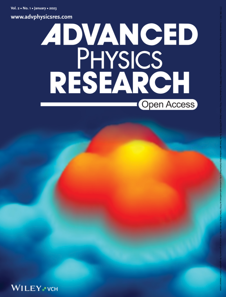
….Whereas STM has been used to study dimers made of bare metal atoms adsorbed on a metal surface, similar studies with molecules are scarce despite their potential interest for applications. IPCMS researchers present an original method to create Mn-Phthalocyanine dimer (MnPc)2 complexes by on-surface assembly. They demonstrate that the dimer can be switched between an antiferromagnetic (AFM) and a ferromagnetic (FM) state upon a small conformational change controlled by STM manipulation. The two states of the molecular switch are easily identified spectroscopically by their Kondo resonance. Experimental results are fully supported by rigorous and exhaustive ab-initio calculations. These findings provide strong arguments for using magnetic dimers as bi-stable molecular switches and open up new research avenues in spintronics, logics and computing at the molecular scale.
This research was highlighted by the editor as the cover page of Advanced Physics Research Journal, Vol. 2, No1, Jan. 2023.
Schematics of the conformational change controlled by STM manipulation: reversible switching between the on-top and shifted configurations of the MnPc dimer by means of the STM tip.
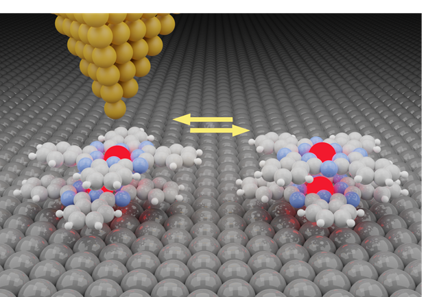
The spatial distribution of spin density in a) On-top and b) Shifted configuration of the MnPc dimer on Ag(111). The on-top configuration of the MnPc dimer couples antiferromagnetically (AFM) through direct exchange, and switches to the ferromagnetic (FM) coupling through super exchange in the shifted configuration. The red and blue colors are representing the spin-up and spin-down density, respectively. The isosurface value is 0.02 eÅ−3.